top of page
PCB Design & Layout
Submit your schematic; our engineers will design the PCB layout, convert to GERBER files, and fabricate.

Design Capability
File Requirements
Schematic Diagram
Component Footprint (including footprint type and dimensional drawing if not provided)
Mechanical Drawing (covering board outline, dimensions, screw/mounting hole locations, fiducial markers, and edge treatment e.g., rounded corners)
Comparison | PCB Design | PCB Layout |
|---|---|---|
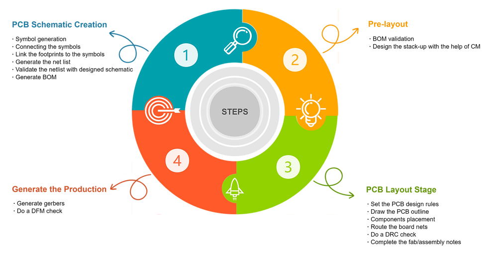
Definition | Schematic Diagram: Design component connection logic | Place & Route: Transform diagrams into physical PCB structures |
Objective | Ensuring correct circuit logic, functional implementation, and proper signal transmission. | Ensuring reasonable structure, clear routing, manufacturability, testability, and performance compliance. |
Key Tasks | Schematic capture | Component placement |
Electrical Rule Check (ERC) | Routing and impedance control | |
Component selection and footprint creation | Power and ground plane planning | |
Signal and power planning | Thermal management design | |
Functional block division | Design Rule Check (DRC) and Gerber file generation | |
Tools/Software | Altium Designer, OrCAD, KiCad, EasyEDA (schematic modules) | Altium Designer, Allegro, PADS, KiCad, Eagle (PCB layout modules) |
Output Deliverables | Schematic files (.Sch) | PCB layout file (.PCB) |
Bill of Materials (BOM) | Gerber files | |
Netlist | Drill files | |
Assembly drawings and outputs | ||
Focus Areas | Functional correctness, proper signal logic, and electrical design integrity. | DFM-Optimized Routing; Signal Integrity (SI); Thermal Management |
Out of gallery
DESIGN
FLOW

bottom of page


